


Applications:
a. Widely used for the inspection of micro-structure of large silicon chip
b. Analysis of bare IC structure and the inspection of defective sample
c. ITO clearance of LCD module and COG observation
d. Observation and analysis of metallographic structure
e. Micro-observation of reflective material
f. Optional 2D/3D manual viewer to inspect SMT solder bead
g. Optional motorized device with super depth of field can 3D display and measure the depth(More detail please contact our technician)
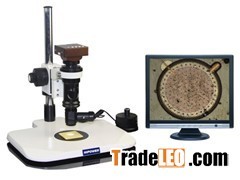
HDM-600 High Resolution Digital Microscope

Shenzhen Hipower Precision Instrument Co., Ltd.
biological microscope, stereo microscope, 2D/3D video microscope, metallog...
